Difference between revisions of "AMD CPUs"
Michael Dale (talk | contribs) |
Michael Dale (talk | contribs) (→K5) |
||
| (11 intermediate revisions by 2 users not shown) | |||
| Line 1: | Line 1: | ||
| + | ==8088/8086/286== | ||
| + | AMD began it's business in the x86 CPU business acting as a second source (under lisence) for Intel. Their 8088s and 8086s are identical to the Intel versions. AMD 80286s were also identical, except that AMD went on to produce 16 and 20MHz versions whereas Intel's fastest 286 was rated at 12.5MHz. | ||
| + | |||
== 386 == | == 386 == | ||
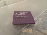
| + | The Am386 CPU was a 100%-compatible clone of the Intel 80386 design released by AMD in 1991. It had been tied up in court for some time, as Intel did not believe AMD had the right to use their microcode. The Am386 is more or less an exact clone of the i386, but was offered in a 40MHz part. The 40MHz part was very affordable and was competitive with Intel's low-end 486 offerings. This is the chip that put AMD on the map. Am386 was made in both 16-bit "SX" and 32-bit "DX" versions. | ||
[[File:AMD_386_DX_40MHz.jpg|200px|thumb|AMD 386DX 40MHz]] | [[File:AMD_386_DX_40MHz.jpg|200px|thumb|AMD 386DX 40MHz]] | ||
== 486 == | == 486 == | ||
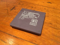
| + | Am486 was release on the market nearly four years after Intel, but AMD continued the tradition of pricing them lower than Intel's which made them popular with enthusiasts and OEMs. The Am486DX, DX2, and SX2 chips gained acceptance among larger computer manufacturers, especially Acer and Compaq, in the 1994 time frame. The 5V am486 chips matched Intel's performance (more or less) on a clock-for-clock basis, but suffered from excessive heat production, especially the 80MHz clock doubled parts. This was later rectified in the 3.3V versions. Although the AMD DX4 chips were not much of a match for the Intel DX4s due to their smaller L1 cache sizes and lack of ALU enhancements. However, unlike Intel, AMD did produce their DX4s in a 120MHz version. AMD's higher clocked 486 chips provided superior performance to many of the early Pentium chips, especially the 60 and 66 MHz parts. While equivalent Intel 80486DX4 chips were priced high and required a minor socket modification, AMD priced low. AMD's DX4-100 usually cost less than Intel's DX2-66. AMD chips were available with either writeback or writethrough L1 caches. | ||
| + | |||
| + | [[File:AMD_486_DX2_80MHz.jpg|200px|thumb||AMD 486 DX/2]] | ||
| + | |||
| + | == 5x86 == | ||
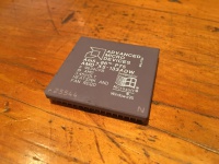
| + | As the K5 fifth generation CPU was not yet ready for market, AMD needed something to compete with Intel's Pentium. The result was the 5x86. It was actually just a clock quadrupled am486 based on a .35 micron 3.3V core with 16kb internal WB/WT cache. All am5x86s were rated for 133MHz, though AMD originally intended to sell 150 and 160MHz versions as well. A few prototypes have been found in the wild. It is not known if they were held back due to problems with the 40 and 50MHz busses or because they would have been too competitive with the K5. The 5x86's very low price made it a favourite of PC enthusiasts, especially as they were easily overclocked. It was generally comparable with the Pentium 75 in terms of integer performance. Many upgrade kits were sold with the 5x86 which made it easy to breathe new life into an aging 486 computer. Despite sharing the same name, the am5x86 has nothing in common with the Cyrix 5x86 chip which uses a true 5th generation design. | ||
| + | |||
| + | [[File:AMD_5x86_133MHz.jpg|200px|thumb||AMD 5x86]] | ||
== K5 == | == K5 == | ||
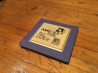
| + | K5 was AMD's first x86 processor to be developed entirely in-house. Introduced in March 1996, it was designed to compete with Intel's Pentium. The K5 was an ambitious design that was closer to a Pentium Pro than the Pentium (actual performance was closer to the Pentium). K5 was based on the 29k RISC processor architecture with an x86 decoding front-end. The K5 was highly compatible. All models had 4.3 million transistors, with five integer units (that could process instructions out of order) and one floating point unit. The branch target buffer was four times the size of the Pentium's and register renaming improved parallel performance of the pipelines. The chip's speculative execution of instructions reduced pipeline stalls. It had a 16 KB, four-way set associative instruction cache and an 8 KB data cache (24kb cache total). The K5 did not include MMX instructions, as MMX had not been finalized by Intel until the following year. There were two sets of K5 processors (SSA/5 and the 5k86). Both were released with the K5 label. The "SSA/5" line ran from 75 to 100 MHz (5K86 P75 to P100, later K5 PR-75 to PR100); the "5k86" line ran from 90 to 133 MHz. However, AMD used what it called a PR rating, or performance rating, to label the chips according to their equivalence to a Pentium of that clock speed. Thus, a 116 MHz chip from the second line was marketed as the "K5 PR166". Manufacturing delays caused the PR200's arrival to nearly align with the release of K6. Since AMD did not want the two chips competing, the K5-PR200 only arrived in small numbers. Ultimately the K5 failed in the marketplace, primarily for being more than a year behind schedule but also due to a week FPU, the questionable "PR" rating system and AMD's inability to produce them at higher clock rates. | ||
| + | |||
| + | [[File:AMD_K5_PR100.jpg|200px|thumb|AMD K5]] | ||
== K6 == | == K6 == | ||
| + | Due to the marketplace failure of the K5, AMD purchased Nexgen to acquire a sixth generation design. K6 began life as the Nexgen 686, but was modified under AMD's supervision to function on a standard Socket 7 Pentium bus. Like the K5 the K6 was heavily based on a RISC design with a CISC front end, and shared at lot in common with Pentium Pro. 32-bit integer performance was indeed competitive with Pentium pro, but it lacked a strong FPU and integrated L2 cache (though it did have a very large 64kb L1 cache). K6 supported MMX, but using a weaker implementation than the Pentium MMX. Despite not being as fast as Pentium II, and even being slower than a Pentium MMX in FPU demanding applications, price and performance were good enough to secure good sales. Initially available in speeds of 166 and 200MHz (2.9V), there were substantial delays in getting the 233MHz (3.2V) part to market due to excessive heat issues. This was to be rectified in the .25 micron voltage reduced version. Unfortunately, the lower power versions also suffered from production delays by which time AMD was lagging pretty far behind Intel in the performance department. The second generation of K6 chips "Little Foot" were released in January 1998 and ran at 200, 233, 266 and 300MHz. All chips ran at 66MHz with a 2.2V core voltage. Like Pentium MMX, all K6 chips used split rail voltage. | ||
[[File:AMD_K6-200.jpg|200px|thumb||AMD K6 200MHz]] | [[File:AMD_K6-200.jpg|200px|thumb||AMD K6 200MHz]] | ||
| Line 15: | Line 31: | ||
Released in early 1998, the K6-2 CPUs were an enhancement of the original K6. Cache size remained the same, however the K6-2 saw the introduction of 3Dnow!, a SIMD instruction set akin to MMX. Some games and drivers (especially 3Dfx) were patched or updated to take advantage of 3Dnow!. Quite a few K6-2 models ran using a 100MHz FSB which gave a boost of 5%-10% depending on the game. | Released in early 1998, the K6-2 CPUs were an enhancement of the original K6. Cache size remained the same, however the K6-2 saw the introduction of 3Dnow!, a SIMD instruction set akin to MMX. Some games and drivers (especially 3Dfx) were patched or updated to take advantage of 3Dnow!. Quite a few K6-2 models ran using a 100MHz FSB which gave a boost of 5%-10% depending on the game. | ||
K6-2 processors are used quite often in Super Socket 7 machines thanks to the unlocked multiplier. Its overall floating point performance, however, was not as high as that of Intel's Pentium II or even Celeron. | K6-2 processors are used quite often in Super Socket 7 machines thanks to the unlocked multiplier. Its overall floating point performance, however, was not as high as that of Intel's Pentium II or even Celeron. | ||
| + | |||
| + | [[File:AMD_K6-2_400MHz.jpg|200px|thumb||AMD K6-2 400MHz]] | ||
== K6-III == | == K6-III == | ||
Latest revision as of 18:04, 22 October 2015
Contents
[hide]8088/8086/286
AMD began it's business in the x86 CPU business acting as a second source (under lisence) for Intel. Their 8088s and 8086s are identical to the Intel versions. AMD 80286s were also identical, except that AMD went on to produce 16 and 20MHz versions whereas Intel's fastest 286 was rated at 12.5MHz.
386
The Am386 CPU was a 100%-compatible clone of the Intel 80386 design released by AMD in 1991. It had been tied up in court for some time, as Intel did not believe AMD had the right to use their microcode. The Am386 is more or less an exact clone of the i386, but was offered in a 40MHz part. The 40MHz part was very affordable and was competitive with Intel's low-end 486 offerings. This is the chip that put AMD on the map. Am386 was made in both 16-bit "SX" and 32-bit "DX" versions.
486
Am486 was release on the market nearly four years after Intel, but AMD continued the tradition of pricing them lower than Intel's which made them popular with enthusiasts and OEMs. The Am486DX, DX2, and SX2 chips gained acceptance among larger computer manufacturers, especially Acer and Compaq, in the 1994 time frame. The 5V am486 chips matched Intel's performance (more or less) on a clock-for-clock basis, but suffered from excessive heat production, especially the 80MHz clock doubled parts. This was later rectified in the 3.3V versions. Although the AMD DX4 chips were not much of a match for the Intel DX4s due to their smaller L1 cache sizes and lack of ALU enhancements. However, unlike Intel, AMD did produce their DX4s in a 120MHz version. AMD's higher clocked 486 chips provided superior performance to many of the early Pentium chips, especially the 60 and 66 MHz parts. While equivalent Intel 80486DX4 chips were priced high and required a minor socket modification, AMD priced low. AMD's DX4-100 usually cost less than Intel's DX2-66. AMD chips were available with either writeback or writethrough L1 caches.
5x86
As the K5 fifth generation CPU was not yet ready for market, AMD needed something to compete with Intel's Pentium. The result was the 5x86. It was actually just a clock quadrupled am486 based on a .35 micron 3.3V core with 16kb internal WB/WT cache. All am5x86s were rated for 133MHz, though AMD originally intended to sell 150 and 160MHz versions as well. A few prototypes have been found in the wild. It is not known if they were held back due to problems with the 40 and 50MHz busses or because they would have been too competitive with the K5. The 5x86's very low price made it a favourite of PC enthusiasts, especially as they were easily overclocked. It was generally comparable with the Pentium 75 in terms of integer performance. Many upgrade kits were sold with the 5x86 which made it easy to breathe new life into an aging 486 computer. Despite sharing the same name, the am5x86 has nothing in common with the Cyrix 5x86 chip which uses a true 5th generation design.
K5
K5 was AMD's first x86 processor to be developed entirely in-house. Introduced in March 1996, it was designed to compete with Intel's Pentium. The K5 was an ambitious design that was closer to a Pentium Pro than the Pentium (actual performance was closer to the Pentium). K5 was based on the 29k RISC processor architecture with an x86 decoding front-end. The K5 was highly compatible. All models had 4.3 million transistors, with five integer units (that could process instructions out of order) and one floating point unit. The branch target buffer was four times the size of the Pentium's and register renaming improved parallel performance of the pipelines. The chip's speculative execution of instructions reduced pipeline stalls. It had a 16 KB, four-way set associative instruction cache and an 8 KB data cache (24kb cache total). The K5 did not include MMX instructions, as MMX had not been finalized by Intel until the following year. There were two sets of K5 processors (SSA/5 and the 5k86). Both were released with the K5 label. The "SSA/5" line ran from 75 to 100 MHz (5K86 P75 to P100, later K5 PR-75 to PR100); the "5k86" line ran from 90 to 133 MHz. However, AMD used what it called a PR rating, or performance rating, to label the chips according to their equivalence to a Pentium of that clock speed. Thus, a 116 MHz chip from the second line was marketed as the "K5 PR166". Manufacturing delays caused the PR200's arrival to nearly align with the release of K6. Since AMD did not want the two chips competing, the K5-PR200 only arrived in small numbers. Ultimately the K5 failed in the marketplace, primarily for being more than a year behind schedule but also due to a week FPU, the questionable "PR" rating system and AMD's inability to produce them at higher clock rates.
K6
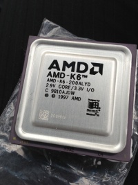
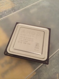
Due to the marketplace failure of the K5, AMD purchased Nexgen to acquire a sixth generation design. K6 began life as the Nexgen 686, but was modified under AMD's supervision to function on a standard Socket 7 Pentium bus. Like the K5 the K6 was heavily based on a RISC design with a CISC front end, and shared at lot in common with Pentium Pro. 32-bit integer performance was indeed competitive with Pentium pro, but it lacked a strong FPU and integrated L2 cache (though it did have a very large 64kb L1 cache). K6 supported MMX, but using a weaker implementation than the Pentium MMX. Despite not being as fast as Pentium II, and even being slower than a Pentium MMX in FPU demanding applications, price and performance were good enough to secure good sales. Initially available in speeds of 166 and 200MHz (2.9V), there were substantial delays in getting the 233MHz (3.2V) part to market due to excessive heat issues. This was to be rectified in the .25 micron voltage reduced version. Unfortunately, the lower power versions also suffered from production delays by which time AMD was lagging pretty far behind Intel in the performance department. The second generation of K6 chips "Little Foot" were released in January 1998 and ran at 200, 233, 266 and 300MHz. All chips ran at 66MHz with a 2.2V core voltage. Like Pentium MMX, all K6 chips used split rail voltage.
K6-2
Released in early 1998, the K6-2 CPUs were an enhancement of the original K6. Cache size remained the same, however the K6-2 saw the introduction of 3Dnow!, a SIMD instruction set akin to MMX. Some games and drivers (especially 3Dfx) were patched or updated to take advantage of 3Dnow!. Quite a few K6-2 models ran using a 100MHz FSB which gave a boost of 5%-10% depending on the game. K6-2 processors are used quite often in Super Socket 7 machines thanks to the unlocked multiplier. Its overall floating point performance, however, was not as high as that of Intel's Pentium II or even Celeron.
K6-III
The K6-III was released in 1999 , just a few months before the Athlon, although only in small volumes. It's only advantage over the K6-2 is the inclusion of full-speed L2 cache on the chip, where as K6 and K6-2 processors used motherboard cache as L2. This has the additional benefit of increasing the cacheable area. This is significant, as many Socket 7 and Super 7 motherboards could only cache 64MB or 128MB (only a few motherboards could cache more memory). When using a K6-III the motherboard cache acts as L3 cache. K6-III processors come in 2 different voltages, namely 2.2V and 2,4V. While the 2.2V parts produce only slightly more heat then the Pentium MMX parts do, the 2.4V chips ran rather hot (about 20W max for the 2.2V part and almost 30W max for the 2.4V part). In terms of performance, certain games such as MDK2 love the full-speed L2 cache and benefit from it, although most games don't benefit nearly as much. K6-III CPUs should generally be avoided and replaced with K6-2+/III+ CPUs (if the motherboard supports it) which are much cooler and clock higher.
K6-2+/K6-III+
K6-2+/K6-III+ CPUs were released in 2000 as cheap upgrades to owners of K6-2 and K6-III CPUs. They were manufactured at a smaller 0.180nm process thus consuming far less power. Despite the name, both processors feature full-speed ondie L2 cache, with the K6-2+ featuring 128KB and the K6-III+ 256KB. The K6-2+/III+ are perhaps the most favoured chips from the K6 line of CPUs, due to their low heat output and minimal power requirements, most of which allow them to clock as high as 600MHz, which generally is an easily attainable speed. At that speed, the performance of the K6-II+/III+ is around that of Pentium II 400 and Pentium III (Katmai) 500, depending on the game.
NOTE
Keep in mind that at speeds greater than 600MHz, most onboard cache (L3 Cache when using K6+ chips) will have to be disabled as it won't be able to cope with the high frequency.
Athlon
In 1999 AMD left Super 7 behind and created the Athlon processor for Slot A. This was a vast improvement when compared to it's earlier offerings and made AMD a genuine competitor to Intel, which started the famous "1GHz race". Later AMD replaced Slot A with Socket A around the time it introduced Athlon's second core, the Thunderbird. Thunderbird at first made use of a 200MHz FSB (using 100MHz SDRAM) but this was later raised to 266MHz (using 133MHz SDRAM). A budget version of Thunderbird was also made, called the Duron. The Duron is basically a Thunderbird with 3/4's of it's L2 cache cut away, yet it still remained competitive compared to Intel's Celeron's. Thunderbird went from 600MHz to 1400MHz.
When AMD introduced Thunderbird's successor, it had to compete with Intel's netburst CPU's, which inherently had much higher clock frequencies compared to Thunderbird. It was then that AMD reinstated the PR rating, starting with Thunderbird's successor, the Palomino.
The Palomino was basically an optimized Thunderbird (something which can be seen as the die is more square compared to the rectangular die of the Thunderbird CPU's) build in the same manufacturing process. Another difference is that Palomino CPU's were made with a plastic package instead of the purple ceramic package used by Thunderbird.
Both Thunderbird and Palomino produced a large amount of heat (sometimes in excess of 70W, compared to the 30W to 35W of Pentium 3) and needed beefy coolers in order to be kept cool and were relatively easy to overheat and burn out if the CPU cooler was either not installed properly or if it had moved while the entire system was in transit (like in the back of a car on a bumpy road). None of the Thunderbirds have internal thermal protection circuitry, thus one has to be very careful when installing the CPU cooler. An internal thermal diode (that shut down the CPU in case of overheating) was introduced with the Palomino, but reliability of that thermal diode is heavily dependent on the motherboard - it often didn't work correctly with lower quality / cheaper motherboards. Video showcasing operation without heatsink
The Palomino is otherwise better known as "Athlon XP" and "Athlon MP" (the latter was designed for use in multiple processor systems) and, as mentioned before, used the PR rating in it's model number instead of using it's real clock speed like Thunderbird did. Palomino was also generally the first Athlon to use DDR memory instead of SDRAM (though both can work with either type of memory, it is best to use DDR memory instead of SDRAM as SDRAM created quite a memory bandwidth bottleneck). Palomino went from 1333MHz (1500+ rating) to 1733MHz (2100+ rating).
Palomino was succeeded by Thoroughbred, which was basically a die-shrink of Palomino and the processor die regained it's rectangular shape. Thoroughbred had some initial problems when AMD tried to scale Thoroughbred and a second revision of Thoroughbred was made to solve that problem successfully. Thoroughbred was also the first Athlon to reach a 333MHz FSB. Thoroughbred scaled from 1400MHz all the way to 2200MHz
Thoroughbred was again succeeded by the Barton core, which doubled the L2 cache from 256KB to 512KB, somewhat improving performance. Barton was also the first Athlon to reach a 400MHz FSB. And even though Barton was barly any faster then the fastest Thoroughbred which it replaced, it still performed better thanks to it's increased L2 cache.
The 2500+ Barton chip was very popular with overclockers as it was often possible to overclock the chip to 3200+ speeds.
Today: Try to get the fastest CPU that will run on your motherboard. Theres basically little difference in heat output between the various models of Socket A Athlons, but the performance difference between the older models and the newer ones is significant. The Thunderbirds are very easy to unlock though, one only needs a pencil. But there are also mobile Socket A Athlons which come unlocked in the first place and may consume somewhat less power then the desktop models. When considering building a Socket A system, one should keep in mind that Socket A Athlons draw a lot of power from the 5V line from the PSU, which is something modern PSU's are having trouble with.
